POWER PLANE EXAMPLES
See Also:
Power Planes and Slots (Tutorial)
Defining a Power Plane on Part of a Layer
To define a partial power plane
- Select the Zone Icon
- Left click the mouse consecutively at each boundary corner of the area you wish the zone to cover (hold down the CTRL key to define a curved segment).
- When complete, assign the zone to a net and configure from the resulting dialogue form
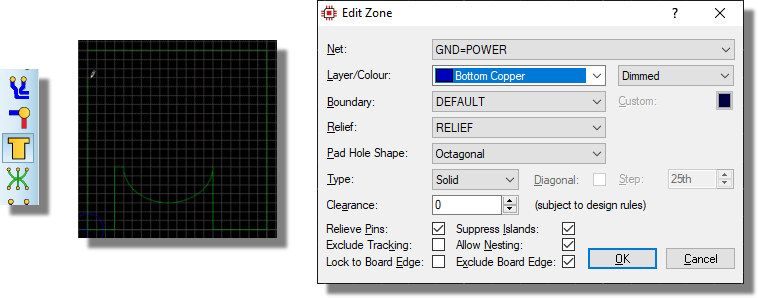
Placing a Power plane
Defining a Keep-Out Area inside a Power Plane
To specify a keep-out area inside a power plane
- Select the Zone Icon
- Left click the mouse consecutively at each boundary corner of the area you wish the keep-out to cover.
- When complete, set the zone type to be EMPTY from the resulting dialogue form
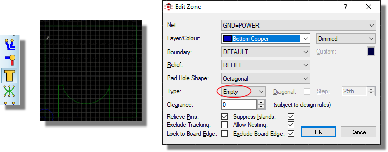
Setting the Zone type to be EMPTY
An empty zone creates an opening in another copper pour on a single layer but is not DRC-enforced. If you need a void beneath a component across multiple copper layers, consider using a DRC room with Exclude Foreign grouped with the component instead. This provides DRC enforcement, covers all the room's layers in a single object, and moves with the component automatically.
Controlling the Copper Flow on a Power Plane
The level of copper coverage is controllable via two options on the Edit Power Plane dialogue form, namely 'Allow Nesting' and 'Suppress Islands'.
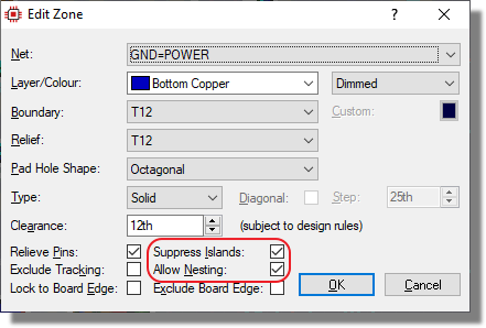
Setting Suppress Islands and Allowing Nesting of the zones
Allow Nesting
When selected the zone will 'jump' over obstacles such as tracks on other nets which would otherwise have prevented the copper flow from entering into an area.
Suppress Islands
When selected all distinct areas of copper which do not connect to a pad on the specified net will be removed.
It follows that maximum zone coverage can be obtained by de-selecting the Suppress Islands option and enable the Allow Nesting option. However, a more common configuration would be to have both Allow Nesting and Suppress Islands enabled.
Specifying a Plane Layer
Specifying a plane layer makes a big difference when it comes to routing the board. In particular, the autorouter will not attempt via connections to planes that are not on a plane layer.
To specify a plane layer
1) Enter the stackup manager on the Technology Menu.
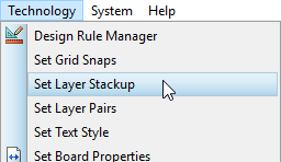
2) Assuming the stackup is correct, change the layer(s) in question from signal to plane.
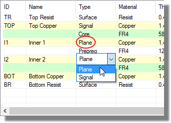
3) It is often a good idea to rename the layers at this stage to reflect their singular purpose.
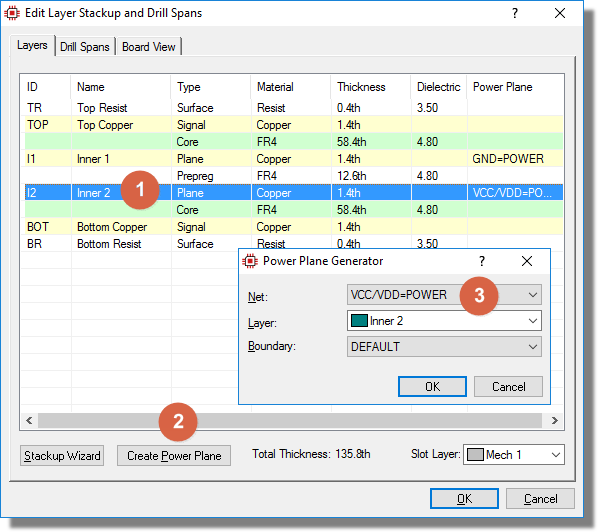
Once created you can add planes to the layer directly from the 'Create Power Plane' button. 1) Select the layer you wish to add a power plane on. 2) Click on the Create Power Plane button. 3) Select the required net and click on OK.
See Also:
Creating a Hatched Zone
Ground and power planes are normally hatched where the resulting board needs to flex.
To create a hatched zone
- Edit the power plane.
- Set the type to be hatched.
- Select the diagonal checkbox for a cross-hatch or mesh topology.
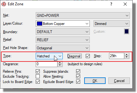
Solid planes are the best return paths. Cross-hatch should only be used when the situation demands it. Trace alignment over cross hatch is then very important and traces should be placed over the cross-hatch intersections.
Finding a Power Plane on the board
On a standard 4 layer board with plane layers this isn't going to be hard. On an 8 layer board with IC specific planes, different grounds and split planes on the other hand it can actually become quite frustrating. The easy way to locate planes is using the Zone Inspector dialogue.
To locate a particular power plane.
- Launch the Zone Inspector dialogue from the Tools menu.
- Select the layer that the zone is on.
- Select the plane from the data grid - it will tag on the editing window.
- Zoom using the button underneath the grid to magnify your view.
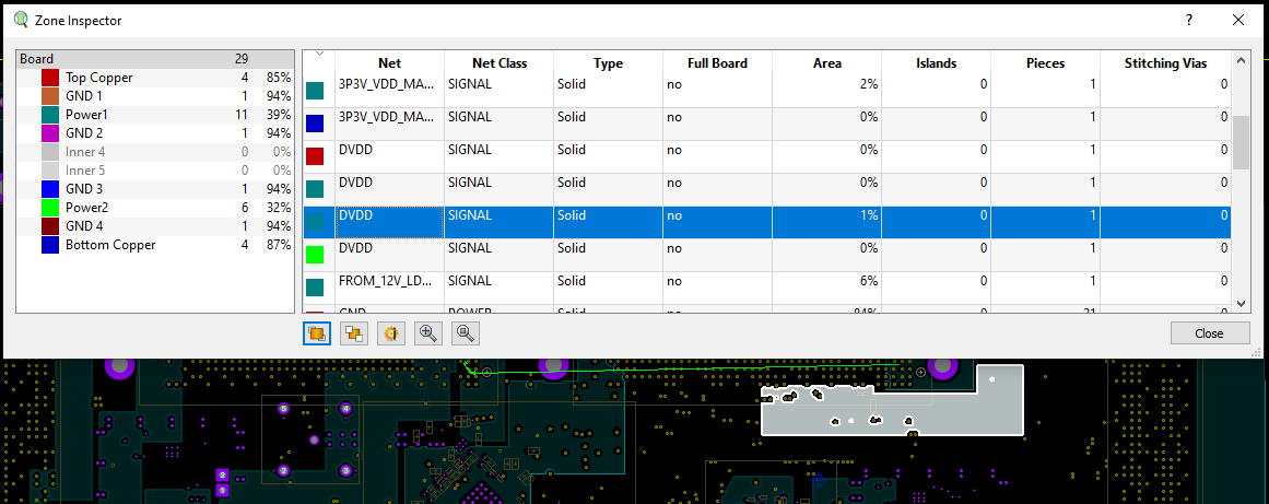
Locating a Power Plane using Zone Inspector. The up and down arrows can be used to switch between planes in the dialogue form.
The zone inspector lists quite a lot of useful information about the plane but if you need to you can edit the plane directly via the button underneath the data grid on the zone inspector dialogue form.
More information on the Zone Inspector can be found here
Specifying the thickness of Thermal Relief used in Power Plane Connections
To define the thermal relief for a power plane
- Edit the power plane
- Change the relief style combo box to the track thickness you wish to be used for relief connections.
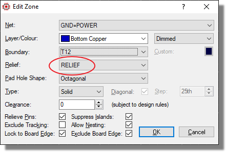
Setting the Relief of the zone to be of style 'Relief'
Note that if the relief style is thicker than the width of a SMT pad then no connection will be made; otherwise there is a danger for design rule violations between the relief track and the surrounding pads on the IC.
The relief style can be up to twice the thickness of the boundary style. Anything thicker than that is rejected, because the relief would begin to 'stick out' past the plane boundary and could cause a short.
It is important to understand that this is the default relief which will be applied to all relevant pads on the zone. You can override this on a per pad basis via the Edit Pad dialogue form (see example below).
A pad whose own relief field is left at Default takes its style from the zone rather than from this setting: the zone's Relieve Pins checkbox decides whether such a pad gets a thermal relief or a solid connection.
Changing the Topology of the Relief Stems on a Pad
It is sometimes useful to change the relief stems from '+' to 'x' in order to maximise connectivity to the zone.
To change the direction of the relief stems for a pad
- Edit the pad on the layout
- Change the relief field to 'Thermal X'.
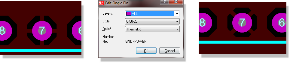
Changing the relief field on a pad to Thermal X to rotate the relief stems
Changing the Topology of the Hole Clearance on a Pad
Sometimes, particularly with hatched zones or flexi-boards, an octagonal hole is less suitable than a more circular approximation.
To define the hole shape on a power plane
- Edit the power plane
- Change the hole shape combo box to the either octagonal or circular.
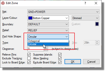
Setting the hole shape on the zone to octagonal or circular
Circular holes are still arc approximated and use the global curve tolerance parameter specified on the Design Rule Manager dialogue form.
Specifying the Clearance for the Power Plane
Key Point: Any border of the power plane is considered to be a trace for design rule purposes
To define the clearance for a power plane
- Go to the Design Rule Manager in the Technology Menu.
- Find or create the design rule that applies to the power plane. This could be the board rule if no other rules have been set up or a layer rule if one has been created for the layer on which the power plane is being placed.
- The Trace->Trace clearance will determine the distance between the power plane and any routes on other nets and the Pad->Trace clearance will determine the clearance between the power plane and any pads/vias on other nets.
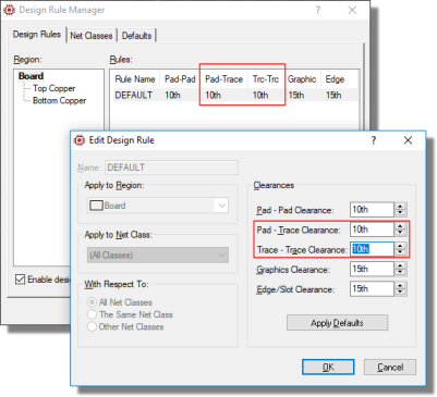
The Pad-Trace and Trace-Trace clearances that govern the plane step off
See Also:
The clearance of the power plane to the board edge is defined by the Edge design Rule.
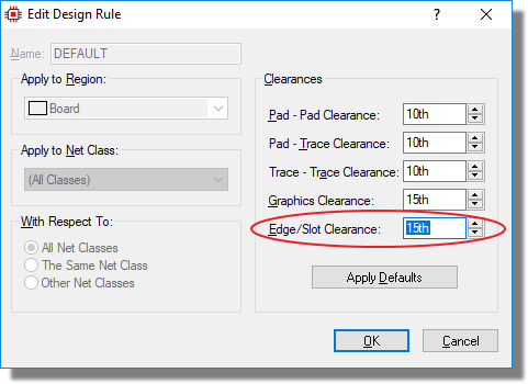
The Edge clearance design rule that sets the plane step off from the board edge
Note that you can also set design rules per layer, meaning that you can specify different clearances for different power planes.
Routing to a Power Plane
If the power plane has been placed on a plane layer then the autorouter will make via connections to the plane wherever possible. Double clicking to place a via during manual routing will also automatically complete the connection to the plane layer.
If the power plane is on a signal layer then the auto-router will not make connections to the plane. Manual connections can be made simply by double clicking the mouse to drop a via or by tracking to the edge of the plane.

Making a manual connection by tracking to the edge of the plane
See Also:
Manual Routing Examples: Routing to a Plane Layer
Setting a Minimum Clearance for a Pad
Normally used for mounting holes, this allows you to set a minimum clearance between power planes and a single pad.
To set a minimum clearance for a pad
- Select pad mode and place a pad of the correct size.
- Right click on the pad, select edit properties and then set the Zone Clearance field as desired.
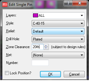
Specifying a minimum 20th clearance from Power Planes on a mounting hole.
Notes:
- The value set is the minimum zone clearance. Actual clearance will be the larger of the design rules, the zone clearance (zone dialogue) and this value.
- If you set the relief style to be solid and the pad is assigned to the same net as a power plane then there will be no clearance between the power plane and the pad, irrespective of the value in the clearance field. The clearance will still apply to all other power planes which are on a different net from the pad.
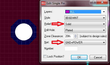
Zone clearance applies to VCC zone on Top Copper but not to GND zone on Bottom because Relief style is set to solid.
Stitching two Power Planes together
Stitching zones is something to be done towards the end of development because it will render the board almost un-routable.
To stitch two power planes together
- Right click on the border of the power plane and select Via Stitch from the resulting context menu.

- If there are multiple planes on different layers select the destination plane for the stitching. Set the via style and the spacings for the via grid.

The Vias group on the dialogue holds the Style, the Drill Range (Smart or Thru-hole), the Via-Via Spacing, a gap field whose label changes with the job in hand, Offset Rows, and Avoid Silkscreen, which keeps the generated vias clear of silkscreen graphics.
The same dialogue is used for all three jobs and its title changes to suit: Stitch Zone when stitching two zones, Shield Zone when shielding a zone perimeter, and Shield Route when shielding a route. That is why the screenshots in the three examples below look slightly different from one another.
Context sensitive help is available on the dialogue form via the '?' at the top right. This contains more information on each field in the dialogue.
3. Exit the dialogue form with the OK button. It may take up to a minute for the zones to be stitched. You will see that vias will appear where they can:
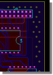
You can remove stitching wholesale via the context menu command on the zone menu or in part by dragging a selection box and changing the selection filter so that only via's are selected. In the latter case be careful not to catch routed via's in the selection.
Via Shield on Power Planes
To place a via shield on power planes
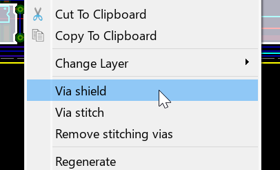
1 To place a via shield around the perimeter of a zone start by right clicking on the zone border and then select via shield from the resulting context menu.
2. Specify the destination zone layer for the stitch (if more than one is available) and then set the spacing requirements for the via placement.
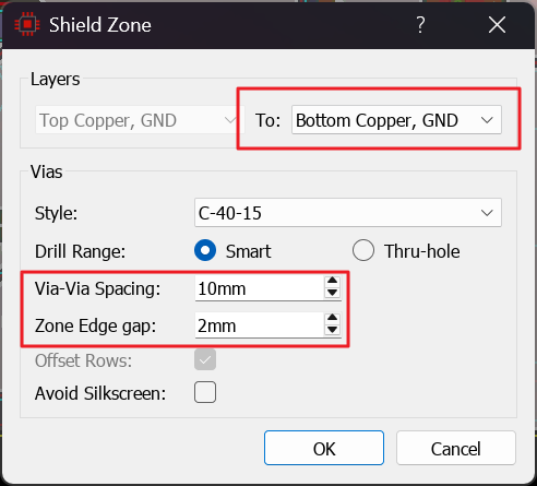
Note that you can use both imperial and / or metric units.
It may take a minute or so to place once you exit the dialogue form.
Shielding a Route with Stitching Vias
To shield a route (or routes) with stitching vias
1. Make sure you have power planes in the correct topology for the shielding vias to be placed. See Stitching and Shielding Zones with Vias.
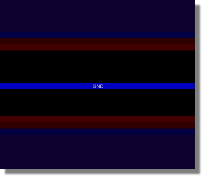
2. Select the route or routes (holding CTRL key down for multiple selection if need be) and then invoke the via shield command from the track context menu. Do not select the zone.
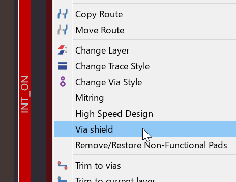
3. You need to specify which two zones are being stitched together and then the spacing between vias and the spacing between the vias and the edge of the route.
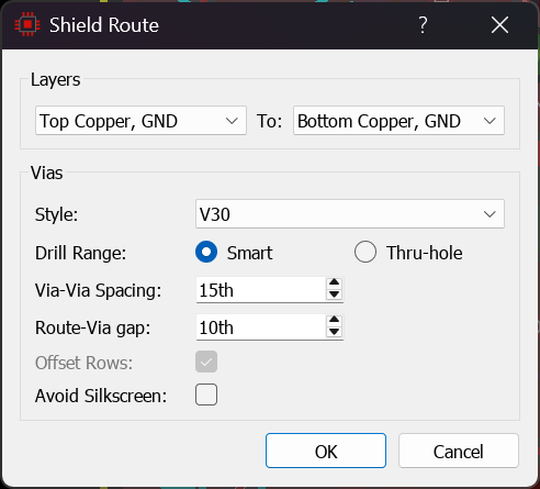
You need to make sure that there are power planes in the right place for the shielding vias to go on.
Joining two Power Planes at a Specific Point
To bridge two power planes at a specific point
- Select track mode and then BRIDGE track style.

- Place a track between the two zones. There is a pop up box that will warn you that the BRIDGE style of track is not electronically connected within the layout.

Note that the BRIDGE track style is, of necessity, outside of the netlist and therefore Proteus will not warn you if you make a mistake. Use with caution!
If you do not have a BRIDGE track style simply create your own trace style and name it BRIDGE.
Placing a BRIDGE track while Follow-Me Routing is active turns Follow-Me Routing off. A second warning tells you this has happened, and you will need to switch the mode back on afterwards if you still want it.
Analysing Power Planes
By far the best way to analyse your use of planes on the board is by using Zone Inspector. You launch this from the Tools menu in the layout module.
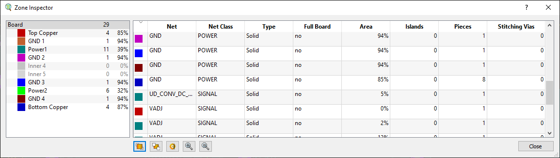
The Zone Inspector Dialogue Form.
The layer info on the left includes number of planes and total coverage on the layer. The main data set on the right shows various plane properties, all of which are explained in more detail in the main help topic.
You can sort the data by column by clicking on a column header at the top. You can sort the columns themselves by dragging and dropping columns around on the data grid. This can be quite helpful if - for example - you want to check how badly your planes have been splintered by placement and routing (order by number of pieces).
You can also use the up and down keyboard arrows to move between the planes in the data grid. This is really helpful if you want to do a visual inspection of the planes on the layout since the editing window view will change to show the currently selected plane.
Finally, you can launch the edit zone dialogue form for the currently selected plane directly via the button underneath the data grid.
Using a Power Plane as a Chassis Bond
Sometimes a copper plane needs to be bonded directly to the chassis of the product, for example to provide EMC shielding or to ground a metal enclosure. In this case, the copper should be exposed (no solder resist covering) so it can make electrical contact when the board is assembled.
To achieve this in Proteus:
- Place a power plane (or zone) on the desired layer and assign it to the ground net or other reference you wish to bond to the chassis.

- Right click on the plane border, select Edit Properties and check the box Open Solder Resist.

- The solder resist opening will cover the entire plane area, leaving the copper bare.

Remember that Open Solder Resist only takes effect on the outer layers and only for a solid or hatched zone; it has no effect on an inner layer plane and is disabled for an Empty zone.
This can also be useful when placing mounting holes or shield can outlines that must make contact with the copper beneath. Pads and holes placed within the exposed plane area will automatically connect.
Be cautious when exposing large plane areas, since bare copper is more prone to oxidation and handling damage. If only certain regions of the plane need to be accessible, restrict the exposed area with polygon editing, or place an exclude foreign design room over the parts you want kept clear, which has the advantage of being DRC enforced across every layer the room covers.